
PCB design and assembly
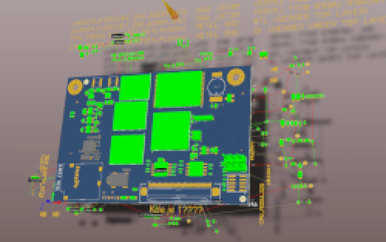
The METEL mark on the device indicates that it is a product developed and manufactured in the Czech Republic — and this also applies to the design of schematics and printed circuit boards, which is 100 per cent our own. Our specialists use Altium Designer for this, which integrates the design of schematics, mechanical layouts and the printed circuit boards themselves, including a comprehensive record of the components used and their documentation.
We apply our own design strategy even to the most demanding tasks — multilayer (up to ten-layer) printed circuit boards for processor modules with BGA packages. As a result, the final hardware is entirely under our control, and our thorough understanding of it enables us to guarantee the correct functioning and safety of every device.
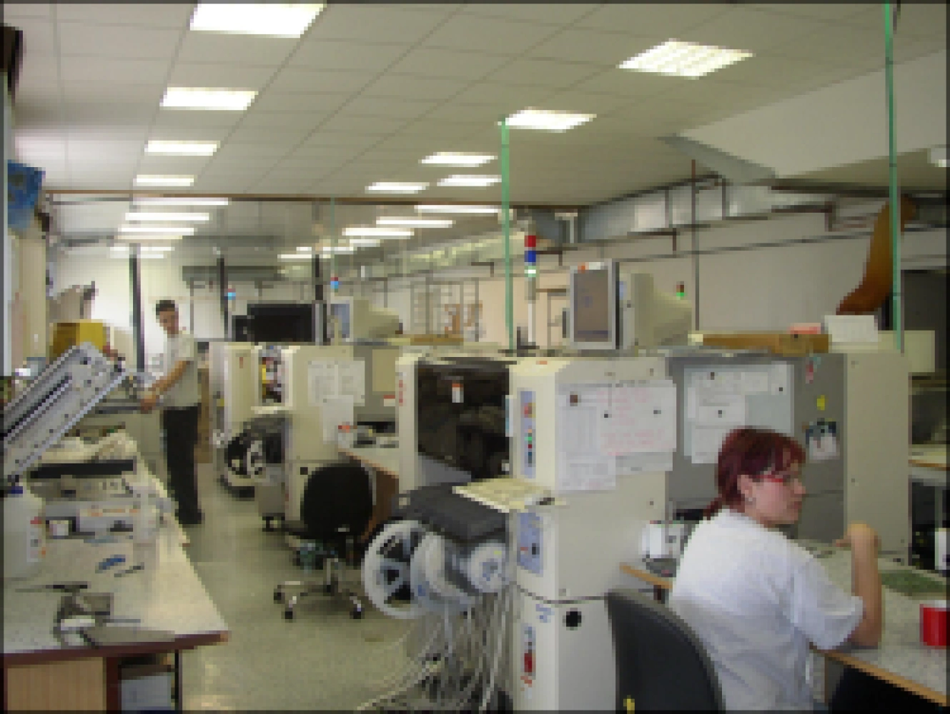
The assembly of printed circuit boards — both prototypes and final production units — takes place at partner companies in the Czech Republic, which are certified to ISO 9001 and comply with IPC, JEDEC, ISO and ČSN standards. We supply key materials from our own warehouse; our partner only adds passive SMD components. Each assembled board then undergoes an optical inspection — and, in the case of boards with BGA packages, an X-ray inspection — before being transported back to our production plant in Česká Skalice for final testing.